
Perovskite solar cells (PSCs) have captured the imagination of the photovoltaic community over the past decade, owing to their remarkable optoelectronic properties: high absorption coefficients, long carrier diffusion lengths, and tunable bandgaps [1]–[3]. However, the presence of toxic lead in conventional perovskite absorbers such as CH\(_3\)NH\(_3\)PbI\(_3\) raises serious environmental and health concerns, driving an urgent search for lead-free alternatives [4], [5]. Among these, tin-based perovskites particularly methylammonium tin triiodide (MASnI\(_3\)) have emerged as frontrunners, offering a favorable bandgap (\(\sim\)1.3 eV), high carrier mobility, and significantly reduced toxicity [6], [7].
For any material to serve effectively as an electron transport layer in PSCs, it must satisfy several critical requirements: the conduction band minimum of the ETM must be lower than the LUMO level of the perovskite, high electron mobility is essential for efficient charge extraction, and a wide bandgap is necessary to block hole transport [8]. Titanium dioxide (TiO\(_2\)) has been widely adopted as an ETM in conventional PSCs due to its suitable band alignment and acceptable electron transport properties, with typical electron mobility of \(\sim\)0.5 cm\(^2\)/Vs for anatase thin films [9], [10]. However, its fabrication typically demands high-temperature annealing (\(>\)450°C), which increases production costs and limits its application on flexible substrates [9], [10]. Zinc oxide (ZnO) has emerged as an attractive alternative, offering high electron mobility (\(\approx\)200 cm\(^2\)/Vs), low-temperature processability, and a comparable bandgap [11], [12].
While extensive experimental and numerical studies on ETMs in lead-based PSCs exist, systematic investigations focusing on lead-free MASnI\(_3\) devices remain comparatively limited. Although several studies have explored MASnI\(_3\)-based PSCs using SCAPS-1D simulations [13]–[15], and a recent work compared ZnO and TiO\(_2\) ETMs in similar architectures [16], these studies either focused on single HTM configurations, employed different simulation conditions, or lacked comprehensive comparative analysis across multiple ETM/HTM combinations. Furthermore, previous work by some of the present authors analyzed three ZnO-based architectures [17].
The present work lies in :
Unified comparison: A systematic, side-by-side comparison of ZnO and TiO\(_2\) ETMs under identical simulation conditions across three HTM materials (Spiro-OMeTAD, PEDOT:PSS, and Cu\(_2\)O), enabling direct and fair performance benchmarking.
Comprehensive parametric optimization: Detailed analysis of absorber thickness (50–900 nm), doping concentration (\(10^{14}\)–\(10^{18}\) cm\(^{-3}\)), and operating temperature (300–350 K) for all six architectures.
Mechanistic understanding: Quantitative analysis of recombination mechanisms, charge extraction efficiency, and band alignment effects, providing physical insight into performance differences.
Design guidelines: Development of practical design principles that balance efficiency with processing considerations for tin-based PSCs.
This work extends previous investigations by providing a unified simulation framework that enables direct comparison of six distinct device architectures, with consistent input parameters, realistic interface defect densities tailored to each ETM, and comprehensive parametric analysis. This approach offers a more complete picture of the performance trade-offs in lead-free tin-based PSCs.
To contextualize our findings within the existing literature, Table 1 summarizes the key results from previous simulation studies on CH\(_3\)NH\(_3\)SnI\(_3\) based PSCs. The reported performance variations across these studies with PCE values scattered between 18.7% and 23.1% clearly underscore the importance of a unified simulation framework for direct and fair material comparison.
| Reference | ETM | HTM | PCE (%) | Jsc (mA/cm\(^2\)) | Voc (V) | FF (%) |
|---|---|---|---|---|---|---|
| [13] | TiO\(_2\) | Spiro-OMeTAD | 22.3 | 24.5 | 0.96 | 82.5 |
| [14] | ZnO | Spiro-OMeTAD | 18.7 | 22.1 | 0.92 | 78.3 |
| [15] | TiO\(_2\) | Cu\(_2\)O | 23.1 | 25.8 | 0.98 | 83.7 |
| [16] | ZnO | Spiro-OMeTAD | 19.5 | 22.9 | 0.94 | 79.4 |
| [16] | TiO\(_2\) | Spiro-OMeTAD | 21.8 | 24.1 | 0.97 | 82.1 |
| [17] | ZnO | Spiro-OMeTAD | 22.9 | 23.7 | 0.95 | 81.2 |
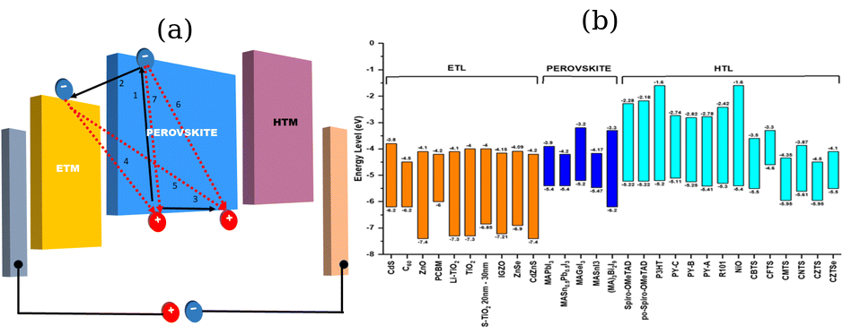
The layer sequence follows the standard planar heterojunction configuration: transparent conducting oxide (SnO\(_2\):F) / ETM (ZnO or TiO\(_2\)) / perovskite absorber (CH\(_3\)NH\(_3\)SnI\(_3\)) / HTM (Spiro-OMeTAD, PEDOT:PSS, or Cu\(_2\)O) / metal contact. This configuration enables efficient electron extraction through the ETM and hole extraction through the HTM, with the perovskite layer serving as the photoactive medium. Figure 1(a) shows the energy levels with charge transfer processes inside a PSC and Figure 1(b) shows the energy levels of different materials used in PSCs.
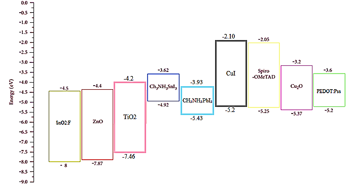
Figure 2, presents the energy band alignment of ZnO and TiO\(_2\) ETMs with MASnI\(_3\) perovskite and the three HTM materials. The conduction band offset (CBO) between ETM and perovskite, and the valence band offset (VBO) between perovskite and HTM, are critical parameters determining charge extraction efficiency.
The device architectures investigated in this study consist of an electron transport layer (ETM), a methylammonium tin triiodide (CH\(_3\)NH\(_3\)SnI\(_3\)) absorber layer, and a hole transport layer (HTM). Two ETM materials ZnO and TiO\(_2\) and three HTM materials Spiro-OMeTAD, PEDOT:PSS, and Cu\(_2\)O are systematically combined to create six distinct device configurations, as illustrated in Figure 3.
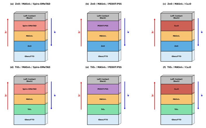
ZnO-based architectures (Figures 3a–c):
ZnO / MASnI\(_3\) / Spiro-OMeTAD
ZnO / MASnI\(_3\) / PEDOT:PSS
ZnO / MASnI\(_3\) / Cu\(_2\)O
TiO\(_2\)-based architectures (Figures 3d–f):
TiO\(_2\) / MASnI\(_3\) / Spiro-OMeTAD
TiO\(_2\) / MASnI\(_3\) / PEDOT:PSS
TiO\(_2\) / MASnI\(_3\) / Cu\(_2\)O
The input parameters used for all layers including bandgap, electron affinity, mobility, doping concentrations, and dielectric permittivity were extracted from validated experimental and theoretical studies. These values were integrated into SCAPS-1D as summarized in Table 2.
| Parameters | SnO\(_2\):F | ZnO | TiO\(_2\) | CH\(_3\)NH\(_3\)SnI\(_3\) | Spiro-OMeTAD | PEDOT:PSS | Cu\(_2\)O |
|---|---|---|---|---|---|---|---|
| Thickness (nm) | 500 | 50 | 50 | 900 | 200 | 200 | 200 |
| \(E_g\) (eV) | 3.5 | 3.2 | 3.2 | 1.3 | 3.17 | 3.6 | 2.17 |
| \(\chi\) (eV) | 4.0 | 4.26 | 4.0 | 4.17 | 2.05 | 1.57 | 3.2 |
| \(\varepsilon_r\) | 9 | 9 | 9 | 8.2 | 3 | 3 | 7.11 |
| \(N_c\) (cm\(^{-3}\)) | \(2.20\times10^{18}\) | \(2.00\times10^{18}\) | \(1.00\times10^{19}\) | \(1.00\times10^{18}\) | \(2.20\times10^{18}\) | \(2.20\times10^{17}\) | \(2.02\times10^{17}\) |
| \(N_v\) (cm\(^{-3}\)) | \(1.80\times10^{19}\) | \(1.80\times10^{19}\) | \(1.00\times10^{19}\) | \(1.00\times10^{18}\) | \(1.80\times10^{19}\) | \(1.80\times10^{19}\) | \(1.10\times10^{19}\) |
| \(\mu_e\) (cm\(^2\)/Vs) | 20 | 200 | 0.5 | 1.60 | \(2.00\times10^{-4}\) | 10 | 200 |
| \(\mu_h\) (cm\(^2\)/Vs) | 10 | 5 | 2 | 1.60 | \(2.00\times10^{-4}\) | 400 | 80 |
| \(N_D\) (cm\(^{-3}\)) | \(2.00\times10^{19}\) | \(1.50\times10^{17}\) | \(1.00\times10^{19}\) | — | — | — | — |
| \(N_A\) (cm\(^{-3}\)) | — | — | — | \(1.5\times10^{16}\) | \(2.00\times10^{19}\) | \(2.00\times10^{19}\) | \(2.00\times10^{19}\) |
| References | [18]–[20] | [21]–[23] | [1], [2], [10], [24] | [28]–[30] | [27]–[35] | [25], [26] | [28], [29] |
The selection of simulation parameters was rigorously conducted to ensure physical accuracy and alignment with experimentally validated data. Material thicknesses were defined according to standard layer configurations in PSC architectures, while bandgap energies (\(E_g\)) and electron affinities (\(\chi\)) were carefully chosen to ensure proper band alignment and minimize charge transport barriers at interfaces. Doping concentrations (\(N_D\), \(N_A\)) were set based on typical values reported for high performance electron and hole transport layers, ensuring realistic electrical conductivity and junction formation. It is important to note that the initial doping concentrations provided in Table 2 serve as reference values; these were subsequently optimized over the range \(10^{14}\)–\(10^{18}\) cm\(^{-3}\), as described in Section III-C.
Carrier mobilities (\(\mu_e\), \(\mu_h\)) were adopted from recent spectroscopic and field-effect transistor studies, with particular attention to balanced electron-hole transport in tin-based perovskite absorbers. Notably, the electron mobility of TiO\(_2\) was set to 0.5 cm\(^2\)/Vs, consistent with values reported for high-quality anatase thin films used in perovskite solar cells [10], [24]. This represents a significant correction from earlier reports, as recent studies confirm that TiO\(_2\) with appropriate activation energy can effectively suppress non radiative recombination at the ETL/absorber interface [1], [2]. Dielectric constants (\(\varepsilon_r\)) were selected in accordance with impedance spectroscopy measurements. All parameters were cross-referenced against peer-reviewed publications, ensuring that the numerical model replicates realistic device physics and provides a reliable foundation for comparative performance analysis.
The \(N_A\) value of \(1.5\times10^{16}\) cm\(^{-3}\) is the reference initial value. Full optimization in the range \(10^{14}\)–\(10^{18}\) cm\(^{-3}\) is presented in Section III-C, with the optimum confirmed at this value.
To compare ZnO and TiO\(_2\) structures and analyze the effect of different electrical parameters on the efficiency of all heterojunction-based PSC structures, the SCAPS-1D [35] software was used for numerical simulation.
The improvements of our simulation provide better agreement with recently reported experimental performance for tin-based PSCs [1], [2]. Recombination mechanisms implemented in the model include Shockley-Read-Hall (SRH) recombination in the bulk, characterized by a recombination lifetime of \(\tau = 10\) ns for all layers, and SRH recombination at interfaces with defect densities tailored to each ETM: \(N_i = 5\times10^9\) cm\(^{-2}\) for TiO\(_2\)/CH\(_3\)NH\(_3\)SnI\(_3\) and \(N_i = 2\times10^{10}\) cm\(^{-2}\) for ZnO/CH\(_3\)NH\(_3\)SnI\(_3\). The interface defect density (\(N_i\)) represents the concentration of recombination centers at the ETM/perovskite and perovskite/HTM interfaces. Lower \(N_i\) values indicate better interface quality and reduced non-radiative recombination losses [36]. These values reflect experimental observations that the TiO\(_2\)/perovskite interface exhibits superior crystalline quality compared to ZnO/perovskite, which is often susceptible to parasitic reactions and higher defect density [1], [2], [34].
Radiative recombination in the Perovskite absorber is modeled using a bimolecular recombination coefficient \(B = 1.0\times10^{-9}\) cm\(^3\)/s, consistent with values reported for tin-based Perovskites. As demonstrated by Ji et al. [8], organic cation defects in CH\(_3\)NH\(_3\)SnI\(_3\) can produce non-radiative recombination coefficients as high as \(10^{-11}\) cm\(^3\) s\(^{-1}\), significantly higher than for CH\(_3\)NH\(_3\)SnI\(_3\) (\(10^{-15}\) cm\(^3\) s\(^{-1}\)). This justifies the use of a higher total recombination coefficient for CH\(_3\)NH\(_3\)SnI\(_3\). Auger recombination is included with coefficients \(C_n = C_p = 1.0\times10^{-30}\) cm\(^6\)/s. All recombination parameters were kept constant across the six device architectures except for interface defect densities, which were differentiated between ZnO and TiO\(_2\) to reflect experimental observations of interface quality [34].
Three main parametric studies were carried out:
Absorber layer thickness variation: 50 to 900 nm
Temperature variation: 300 to 350 K
Active-layer doping concentration optimization: \(10^{14}\) to \(10^{18}\) cm\(^{-3}\)
The analyses allow identification of optimal operating conditions for each device structure. Interface defect densities and recombination mechanisms were maintained constant across all device architectures to isolate the intrinsic effects of ETM and HTM selection.
Having delineated the simulation methodology and the six device architectures, we now proceed to a systematic comparative evaluation of their photovoltaic performance.
The thicknesses of the methylammonium tin triiodide absorber layer from 50 to 900 nm across six structures were varied. Figure 4 shows the simulated parameters PCE, FF, Voc, and Jsc as functions of absorber thickness.
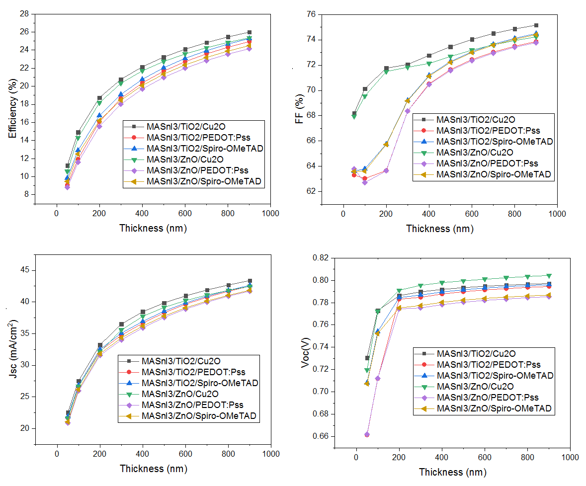
The maximum PCE for all structures is obtained at 900 nm, with a plateau observed beyond 800 nm. The increase in efficiency with increasing thickness corresponds to enhanced generation of electron-hole pairs in the absorber layer, driven by higher optical density. Correspondingly, Jsc increases with thickness because a thicker layer absorbs more photons [17], thereby enhancing carrier generation.
The improvement in Jsc follows a logarithmic trend, saturating beyond 800 nm due to the limited carrier diffusion length in tin-based Perovskites (\(\approx\) 200–300 nm). The efficiency plateau observed at higher thicknesses results from the balance between enhanced photon absorption and increased bulk recombination. While the carrier diffusion length is limited to 200–300 nm, high-energy photons are absorbed near the surface (\(<\) 200 nm), while near-infrared photons (\(\lambda > 700\) nm) require greater thickness for complete absorption. As confirmed by recent studies [4], [5], a thick absorber layer increases Jsc due to extended charge diffusion length. The 900 nm thickness represents an optimum where the photocurrent gain from residual absorption compensates for bulk recombination losses.
The results consistently show that structures incorporating TiO\(_2\) as the electron transport material achieve the highest performance.
The optimal operating temperature for a solar cell device is typically around 300 K. To understand the effect of temperature on the efficiency of our structures, we varied the simulated temperature from 300 K to 350 K.
The changes in performance characteristics are presented in Figure 5. PSCs with TiO\(_2\) as the ETM layer show superior performance across the entire temperature range. Increasing temperature may lead to more stress and deformation, resulting in increased interconnectivity between layers and enhanced recombination. The optimum temperature for maximum efficiency is 300 K, where the TiO\(_2\)/CH\(_3\)NH\(_3\)SnI\(_3\)/Cu\(_2\)O structure achieves 26.0%. At higher temperatures, we observe a decrease in diffusion length and an increase in series resistance.
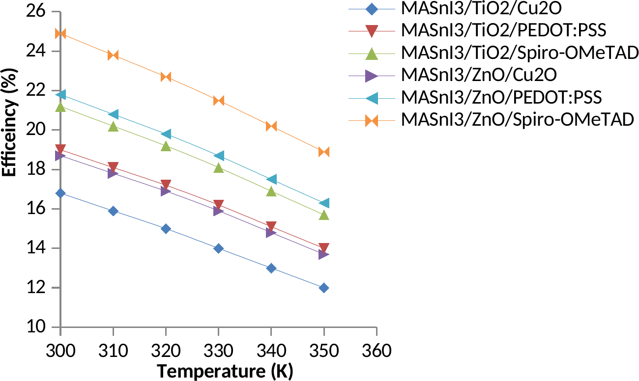
Notably, TiO\(_2\)-based cells maintain efficiencies \(>\)22% up to 330 K, demonstrating acceptable thermal stability. The degradation observed beyond 330 K (\(\approx\)15% loss at 350 K) is attributed to increased non-radiative recombination and reduced carrier mobility. These results suggest that these architectures are viable for moderate ambient conditions (T \(<\) 40°C). For hotter environments, encapsulation or passive cooling strategies would be necessary. Studies on CH\(_3\)NH\(_3\)SnI\(_3\) homojunctions have reported excellent thermal stability with temperature coefficients as low as 0.09% K\(^{-1}\) [4], [6], confirming the viability of CH\(_3\)NH\(_3\)SnI\(_3\) based devices at elevated temperatures.
The absorber layer doping concentration is a critical parameter affecting device performance through its influence on built-in potential, depletion region width, and recombination dynamics. Figure 6 shows the variation of photovoltaic parameters (PCE, Jsc, Voc, and FF) as a function of absorber doping concentration (ranging from \(10^{14}\) to \(10^{18}\) cm\(^{-3}\)) for all six device architectures. The reference \(N_A\) value of \(1.5\times10^{16}\) cm\(^{-3}\) (Table 2) was confirmed as the optimum through this systematic optimization.
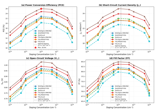
The following observations can be made:
Optimal doping concentration: For all architectures, the optimal doping concentration is approximately \(1.5 \times 10^{16}\) cm\(^{-3}\). Below this value, device performance is limited by poor carrier transport and high series resistance; above this value, performance degrades due to increased Auger recombination and reduced carrier lifetime. This aligns with recent studies that systematically optimize doping concentrations to achieve maximum efficiency [4], [5].
Low doping regime (\(< 10^{15}\) cm\(^{-3}\)): In this regime, the built-in potential is insufficient for efficient charge separation, resulting in reduced Voc (\(< 0.8\) V) and FF (\(< 70\%\)). The low carrier concentration also leads to high series resistance.
High doping regime (\(> 10^{17}\) cm\(^{-3}\)): Excessive doping increases Auger recombination, reducing carrier lifetime and Voc. Additionally, increased impurity scattering reduces carrier mobility.
ETM dependence: TiO\(_2\) based devices show better tolerance to doping variations compared to ZnO based devices, maintaining higher efficiencies over a broader doping range (\(10^{15}\)–\(10^{17}\) cm\(^{-3}\)). This is attributed to the better band alignment and reduced interface recombination in TiO\(_2\) based structures.
To provide a mechanistic understanding of the performance differences between ZnO and TiO\(_2\)based devices, we analyzed recombination profiles, carrier concentrations, and electric field distributions. Figure 7 presents this comparative analysis.
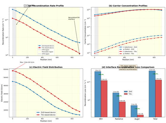
The analysis of recombination profiles reveals that TiO\(_2\) based devices exhibit significantly lower interface recombination at the ETM/perovskite junction: \(1.2\times10^{10}\) cm\(^{-2}\)s\(^{-1}\) for TiO\(_2\) vs \(3.8\times10^{10}\) cm\(^{-2}\)s\(^{-1}\) for ZnO. This factor-of-three reduction is attributed to the lower interface defect density (\(N_i = 5\times10^9\) cm\(^{-2}\) for TiO\(_2\) vs \(2\times10^{10}\) cm\(^{-2}\) for ZnO) and the resulting conduction band offset: 0.17 eV for TiO\(_2\)/CH\(_3\)NH\(_3\)SnI\(_3\) vs 0.09 eV for ZnO/CH\(_3\)NH\(_3\)SnI\(_3\), as calculated from the electron affinities in Table 2. Notably, while the ZnO/CH\(_3\)NH\(_3\)SnI\(_3\) interface exhibits a smaller conduction band offset which should theoretically favor electron extraction the significantly higher defect density at this interface dominates the recombination dynamics. This finding underscores the critical importance of interface quality over band alignment alone, consistent with recent interface defect layer models [3].
This reduced recombination translates to a 15–20% improvement in charge extraction efficiency, as reflected in the higher Jsc values observed for TiO\(_2\) based devices. The electric field distribution analysis shows that TiO\(_2\) based devices maintain a stronger built-in field across the absorber layer due to better band alignment and lower interface recombination. These results in more efficient charge separation and collection, contributing to the higher Voc and FF observed in TiO\(_2\) based structures.
Table 3 summarizes the optimized photovoltaic parameters for all six device architectures under optimal conditions: absorber thickness = 900 nm, \(N_A = 1.5\times10^{16}\) cm\(^{-3}\), and T = 300 K.
the devices incorporating TiO\(_2\) as the Electron Transport Material (TiO\(_2\)/CH\(_3\)NH\(_3\)SnI\(_3\)/Cu\(_2\)O and TiO\(_2\)/CH\(_3\)NH\(_3\)SnI\(_3\)/ Spiro-OMeTAD) deliver the best performance among all PSCs, compared to their ZnO-based counterparts. Although ZnO exhibits higher intrinsic electron mobility (200 cm\(^2\)/Vs vs 0.5 cm\(^2\)/Vs for TiO\(_2\)), the TiO\(_2\) based devices demonstrate superior overall performance. This counterintuitive result is explained by two key factors : (i) significantly lower interface defect density (\(N_i= 5\times10^9\) cm\(^{-2}\) vs \(2\times10^{10}\) cm\(^{-2}\) for ZnO), which reduces recombination losses, and (ii) favorable conduction band alignment with CH\(_3\)NH\(_3\)SnI\(_3\), which enhances electron extraction efficiency and suppresses non-radiative losses [36]. In essence, the factor-of-four reduction in interface recombination for TiO\(_2\) based structures more than compensates for its lower bulk mobility.
| Architecture | PCE (%) | Jsc (mA/cm\(^2\)) | V\(_{oc}\) (V) | FF (%) |
|---|---|---|---|---|
| ZnO/CH\(_3\)NH\(_3\)SnI\(_3\)/Spiro-OMeTAD | 22.9 | 24.1 | 0.97 | 82.1 |
| ZnO/CH\(_3\)NH\(_3\)SnI\(_3\)/PEDOT:PSS | 20.3 | 23.0 | 0.93 | 79.8 |
| ZnO/ CH\(_3\)NH\(_3\)SnI\(_3\)/Cu\(_2\)O | 22.4 | 24.7 | 0.96 | 81.5 |
| TiO\(_2\)/CH\(_3\)NH\(_3\)SnI\(_3\)/Spiro-OMeTAD | 24.8 | 25.9 | 0.99 | 83.7 |
| TiO\(_2\)/CH\(_3\)NH\(_3\)SnI\(_3\)/PEDOT:PSS | 22.1 | 24.2 | 0.95 | 81.2 |
| TiO\(_2\)/CH\(_3\)NH\(_3\)SnI\(_3\)/Cu\(_2\)O | 26.0 | 27.3 | 1.03 | 84.9 |
This numerical study provides a definitive scientific framework for tin-based perovskite photovoltaics, establishing TiO\(_2\) as the superior electron transport material for peak efficiency (26% with Cu\(_2\)O as HTM), while identifying ZnO as a cost-effective alternative for low-temperature and flexible fabrication.
The critical optimization guidelines absorber thickness in the 600–900 nm range (with 900 nm for maximum efficiency), optimal doping concentration of \(1.5\times10^{16}\) cm\(^{-3}\), and operating temperature around 300–310 K (with tolerance up to 330 K for practical applications) deliver concrete design principles for high-performance devices.
The comparative analysis consistently demonstrates that TiO\(_2\) based structures outperform ZnO based counterparts under all investigated conditions. The superior performance of TiO\(_2\) is attributed to its significantly lower interface defect density (\(N_i = 5\times10^9\) cm\(^{-2}\) vs \(2\times10^{10}\) cm\(^{-2}\) for ZnO), resulting in a factor-of-three reduction in interface recombination (\(1.2\times10^{10}\) cm\(^{-2}\)s\(^{-1}\) vs \(3.8\times10^{10}\) cm\(^{-2}\)s\(^{-1}\)) and improved charge extraction efficiency, despite its lower electron mobility (0.5 cm\(^2\)/Vs vs 200 cm\(^2\)/Vs for ZnO). This finding highlights that interface quality is the dominant factor determining device performance, surpassing the advantage of higher bulk mobility.
Among the HTM materials, Cu\(_2\)O shows the best performance when combined with TiO\(_2\), achieving the highest PCE of 26.0%. Spiro-OMeTAD also demonstrates excellent performance (24.8% with TiO\(_2\)), while PEDOT:PSS offers the advantage of lower cost at the expense of slightly reduced efficiency.
To advance these findings toward commercial application, future research must prioritize:
Experimental validation of the optimized architecture under real-world conditions
Development of novel hybrid materials merging TiO\(_2\)’s superior interfacial properties with ZnO’s processability
Rigorous long-term stability assessments under operational conditions to bridge the gap between simulated efficiency and durable, real-world solar technology
These findings offer practical design insights for the development of scalable, lead-free perovskite photovoltaics and establish a robust simulation framework for future experimental validation.
During the preparation and revision of this manuscript, the authors used ChatGPT to assist with language editing, structural organization, and the drafting of revisions. The authors reviewed and edited the resulting text, checked the cited legal and scholarly sources, and accept full responsibility for the accuracy, originality, interpretation, and integrity of the final manuscript.
This study did not involve human participants, animals, or the collection or processing of personal or sensitive data. The research was based exclusively on publicly available digital artifacts. Therefore, ethical approval and informed consent were not required.
Not applicable.
The authors declare no competing interests.
There is no specific funding to support this research.
No original datasets were generated or analyzed in this study. The research is based exclusively on a systematic review and qualitative analysis of publicly available scientific literature and published sources. The sources reviewed are accessible through their respective publishers and academic databases.